Rising Demand for Precision Chemicals Driven by Advanced
Miniaturization Processes
Development of Organic Hardmask Process (Also known as “spin-on hardmask” process at Samsung Electronics) The world’s first development and patent filing of the organic hardmask process and materials, which are essential for next-generation semiconductor manufacturing. Initiated in 2003, this technology must continue to be used by SK hynix and Samsung Electronics for both current and future semiconductor production. Patent filed and registered in 2005 (Application No. 10-2005-0014889, Registration No. 10-0787352)
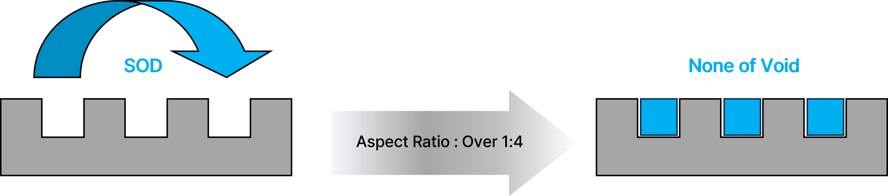
SOD (Spin-On Dielectric) is a gap-fill material used in semiconductors for STI, IMD, and PMD applications, serving as an inter-cell and interlayer insulating film to prevent electrical interference.As device geometries continue to shrink, the presence of microscopic voids in insulating layers can cause gate shorts, making the role of insulation materials increasingly critical.Traditional CVD-deposited insulating materials are now being replaced by spin-on dielectric processes, and materials are being researched to suit this coating method.Polysilazane-based SOD, developed with great care by NEOPATEM, is poised to take a leading role in the semiconductor manufacturing industry's gap-filling technology sector.
Replacement CVD Gap fill Layer by spin coater
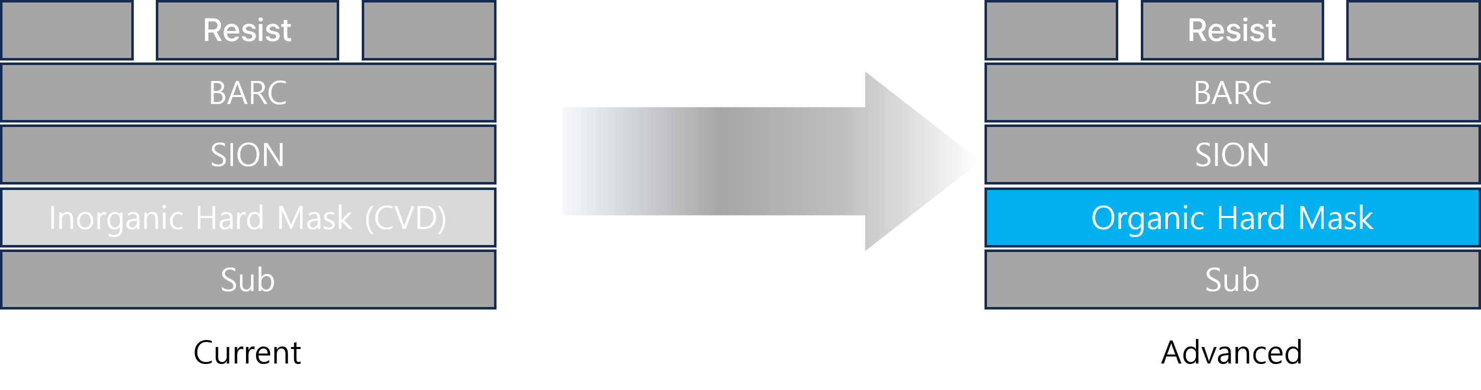
Enhancing Productivity Through Simplified Semiconductor Manufacturing and Low-Energy, High-Efficiency Processing. In the semiconductor industry, fine patterns are typically formed through multilayer structures using chemical vapor deposition (CVD) processes. The spin-on amorphous carbon material developed by our company serves as a hard mask in ArF PR etching processes to prevent damage to Si patterns. It was designed to replace the amorphous carbon layers formed by conventional CVD. Since SiON deposition in semiconductor processing is performed at temperatures exceeding 400 °C, our material was developed to withstand up to 600 °C, making it suitable for high-temperature environments—an advantage that cannot be easily replicated by competitors. Furthermore, it enables mass production and utilizes a simple spin coating process to form the hard mask. By using siloxane compounds as a base and adding crosslinking agents and additives to control optical, thermal, and surface properties, we have improved the etch selectivity between the hard mask layer and the photoresist. The result is a highly functional hard mask layer optimized for spin-coating processes.
Replacement of CVD Hard Mask Layer by spin coater
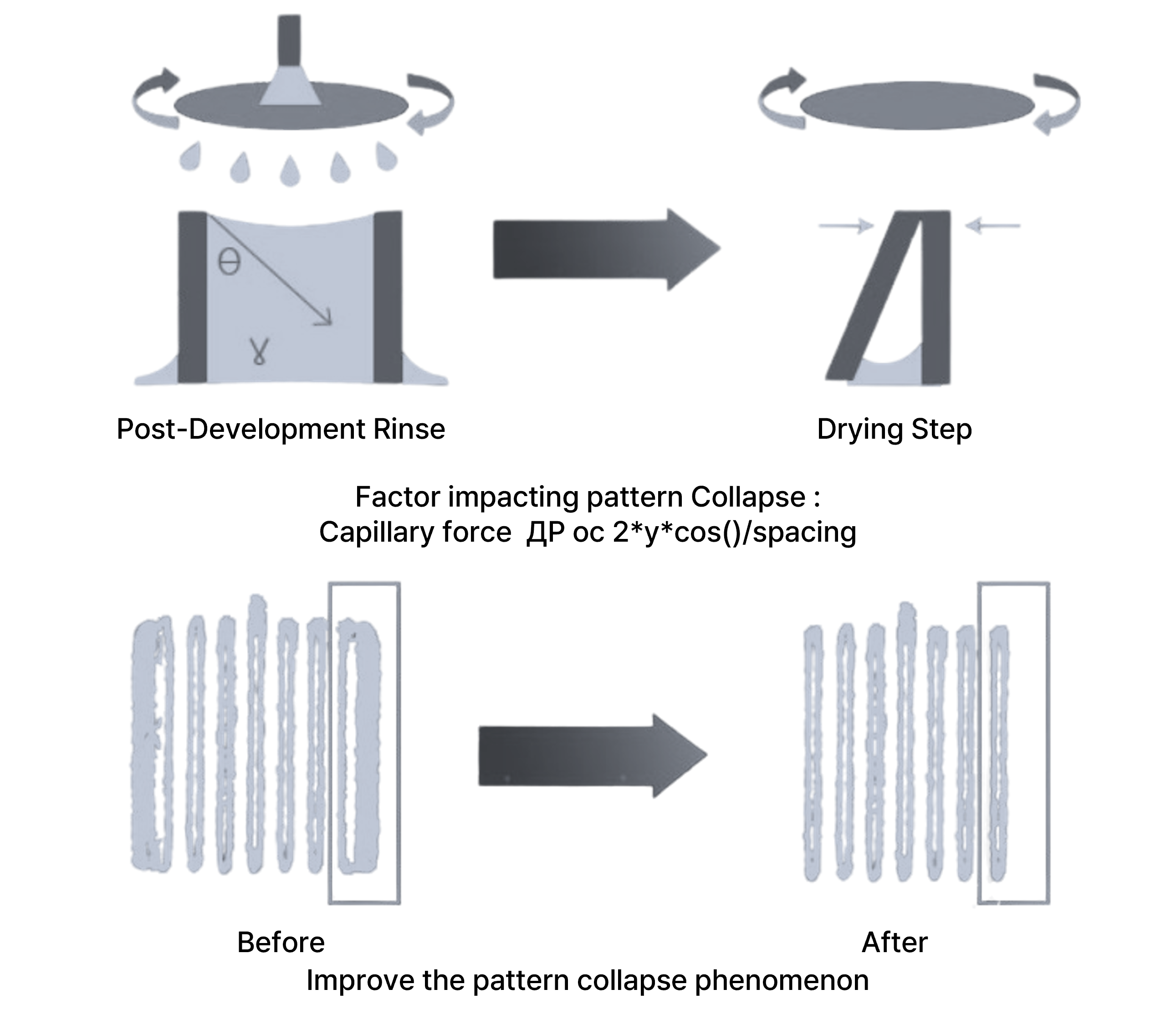
The high-purity surfactant cleaning solution developed by our company is designed for semiconductor device fabrication and possesses low surface tension to address pattern collapse and particle defects caused by the surface tension of DI water during the rinse process after development, especially as patterns become increasingly miniaturized. In general, when forming ultra-fine patterns of 70 nm or smaller, the photoresist layer must be thinned to less than 200 nm to prevent pattern collapse. The photoresist used with 193 nm exposure equipment is typically aliphatic-based, which lacks sufficient etching resistance. As a result, after etching the underlying layers such as poly, metal, or SiO₂, deformation occurs, rendering semiconductor manufacturing unfeasible. Additionally, as the pattern becomes finer, uniformity decreases, which can cause defects in semiconductor devices. To counter this, thicker photoresist layers are required. However, in standard development processes where water is used as the final rinse, the surface tension of water causes pattern collapse. Therefore, a final rinse using a cleaning solution containing surfactants is a more effective alternative. Our cleaning solution dissolves fatty acid alkanolamide-based surfactants in ultrapure water to significantly reduce surface tension, thereby preventing pattern collapse. To minimize turbidity and particle-induced defects, the most critical component, the surfactant, is uniquely structured and synthesized in-house. Furthermore, we apply a proprietary preservative developed internally, mixing it with the formulation during manufacturing. These substances are Nonylphenol-Free, making the product environmentally friendly and compliant with eco-labeling standards.
Replacement of CVD Hard Mask Layer by spin coater
TAG series (Thermal Acid Generator)
In the semiconductor device manufacturing process, photoresists are formulated with thermal acid generators (TAGs) to address the issue of pattern width slimming. After the development process, the patterned structure is subjected to an additional baking step, during which the thermal acid generator releases acid. This acid induces a cross-linking reaction in the photoactive compound, effectively preventing the reduction in pattern width after formation.

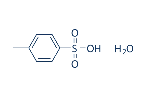
p-Toluenesulfonic acid
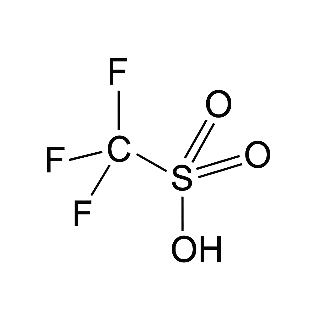
Trifluoromethanesulfonic acid
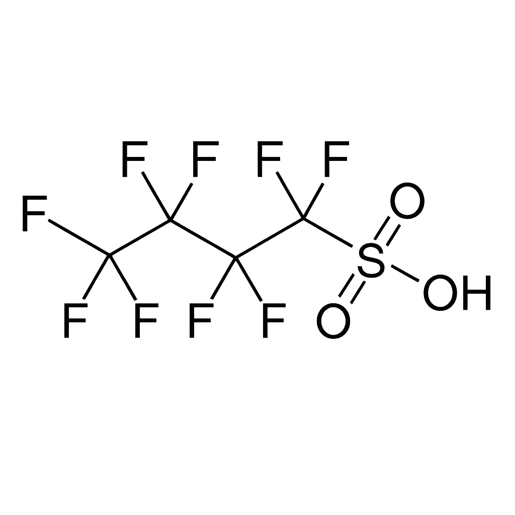
Perfluorobutanesulfonic acid
ST-PAG series (Photo Acid Generator)
To enable ultra-high-resolution microfabrication of semiconductor devices, high-sensitivity chemically amplified photoresists are used.These resists mainly consist of acid-reactive polymers and photoacid generators. Upon exposure to ultraviolet light, organic sulfonate esters undergo photodecomposition to generate strong acids. These acids act as catalysts, reacting with the acid-reactive polymers to initiate chain reactions that cause extensive chemical bonding or decomposition. The generated acid continues to act as a catalyst during the post-exposure bake (PEB) step, amplifying the chemical reactions and creating significant differences in solubility.

Chemical Name: Triphenylsulfonium triflate
Cas no.: 66003-7
- Typical Characteristics:
Appearance: white crystals
Molar mass: 412.45 g/mol
Melting point: 132–134 °C
Imax=233 nm (e=18,000)
e248nm=13,400
Chemical Name: Triphenylsulfonium perfluoro-1-butanesulfonate
Cas no.: 144317-44-2
- Typical Characteristics:
Appearance: white crystals
Molar mass: 562.47 g/mol
Melting point: 82–83 °C
Imax=233.6 nm (e=18,200)
e248nm=13,400
Chemical Name:
Cas no.: –
- Typical Characteristics:
Appearance: white crystals
Molar mass:
? g/mol
Melting point: ? °C
Imax=233 nm (e=?)
e248nm=?